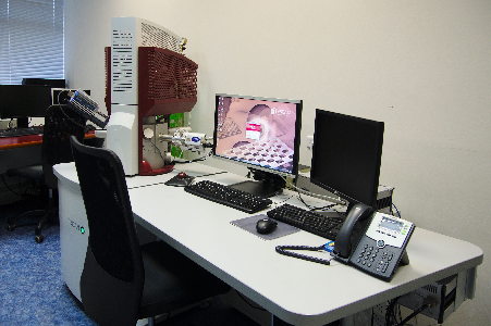
High Resolution Field Emmision Scanning Electron Microscope (FESEM)
Charles University in Prague

A Scanning Electron Microscope (SEM) is a type of electron microscope that produces images of a sample by scanning it with a focused beam of electrons. The electrons interact with atoms in the sample, producing various signals that can be detected and that contain information about the sample’s surface topography and composition. The electron beam is generally scanned in a raster scan pattern and the beam’s position is combined with the detected signal to produce an image. A SEM can achieve a resolution better than 1 nanometer. Specimens can be observed in high vacuum, in low vacuum and in a wide range of cryogenic or elevated temperatures. The most common SEM mode is detection of secondary electrons emitted by atoms excited by the electron beam. The number of secondary electrons that can be detected depends, among other things, on the angle at which the beam meets the surface of the specimen, i.e., on the specimen topography. By scanning the sample and collecting the secondary electrons with a special detector, an image displaying the topography of the surface is created.
The FESEM uses a field emission gun as electron source. Compared to a conventional SEM, it produces clearer, less electrostatically distorted images, with a spatial resolution down to 1.5 nm. FESEM applications include, e.g., semiconductor device cross section analyses for gate widths, gate oxides, film thicknesses and construction details, as well as advanced coating thickness and structure uniformity determination and small contamination feature geometry and elemental composition measurement.
Contacts:
Iva Matolínová (tel:+420-95155-2241)
Ivan Khalakhan (tel. +420 95155 2321)
Technical specifications
Magnification 30 kV:
3.5x – 1,000,000x (for 5’’ image width in Continual Wide Field / Resolution mode)
Resolution:
Between 1.2 nm and 4.5 nm (depending on configuration and accelaration voltage)
Maximum field of view:
70 mm (in basic SE configuration) and 55 mm (with In-Beam SE)
Scanning speed:
From 20 ns to 10 ms per pixel adjustable in steps or continuously
Sample requirements
The samples must be high vacuum stable and conductive. Electrically non-conducting samples must be coated with metal or carbon for imaging. The sample height must not exceed 81 mm (without rotation stage), 60 mm (with rotation stage) and 50 mm (with BDT rotation stage).
Detailed information can be found on the instrument’s webpage.
-
20.02.2025
X-ray computed tomography (CT) TomoLab
-
23.01.2025
THz beamline TeraFERMI


